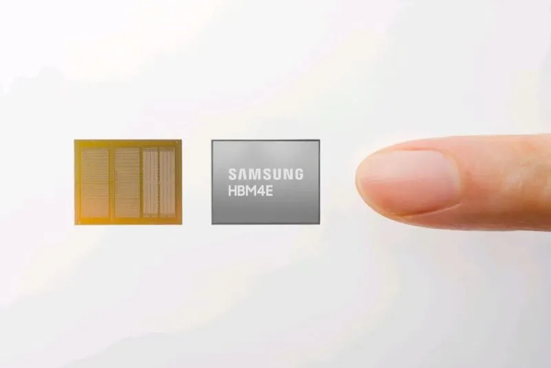
Samsung Electronics will use TSMC's 3-nanometre manufacturing process to produce the base die for Nvidia's next-generation custom high-bandwidth memory, the Seoul Economic Daily reported on Sunday, in a story relayed by Reuters. The arrangement would mark the first time Samsung has worked with the Taiwanese contract chipmaker at the HBM manufacturing stage, and it signals how far Nvidia's push for a standardized memory design now reaches into its suppliers' factories.
High-bandwidth memory, the stacked memory that sits beside AI processors in data centers, is built from DRAM core dies piled on top of a base die, a logic chip that functions as a system semiconductor and manages the flow of data between the memory stack and the processor. Samsung has until now produced both the core die and the base die itself for all of its HBM supply, a turnkey approach that kept the entire product inside its own plants.
That approach is changing for one product. Nvidia has asked Samsung, SK hynix and Micron, the three suppliers tapped to produce its custom memory design known as NVHBM, to manufacture the base die using TSMC's 3-nanometre process, industry sources told the newspaper. Nvidia also requested that the core die be standardized on the sixth-generation DRAM process, known as 1c. NVHBM, unveiled in August, is based on the architecture of HBM4E, the seventh-generation version of HBM, and integrates Nvidia's custom memory controller into the base die.
The request is about consistency. Differing manufacturing methods across HBM suppliers make it difficult to deliver consistent performance from a single design, and standardization also reduces the burden of validating each supplier's product separately. Samsung's Device Solutions division, which runs the company's foundry business, decided after an internal review to accept Nvidia's requirements.
Samsung is not abandoning the turnkey model. The company applies its own 4-nanometre foundry process to the base die of HBM4, which it began mass-producing earlier this year, and of HBM4E, now in mass-production validation, with core dies made on 1c lines at its Hwaseong and Pyeongtaek campuses. It plans to keep the same approach for standard HBM and for custom HBM supplied to other customers, including AMD. Samsung and TSMC did cooperate four years ago to ensure HBM compatibility with TSMC's packaging process, but they have never partnered at the manufacturing stage itself.
Samsung has also kept a hedge in place. The company is validating whether its own foundry can produce the NVHBM base die as well, an industry official told the newspaper, in case demand for the memory exceeds TSMC's production capacity. For now, though, the headline stands: to build Nvidia's next custom memory, the world's largest memory maker will put a core component of its flagship product through its biggest rival's factories.